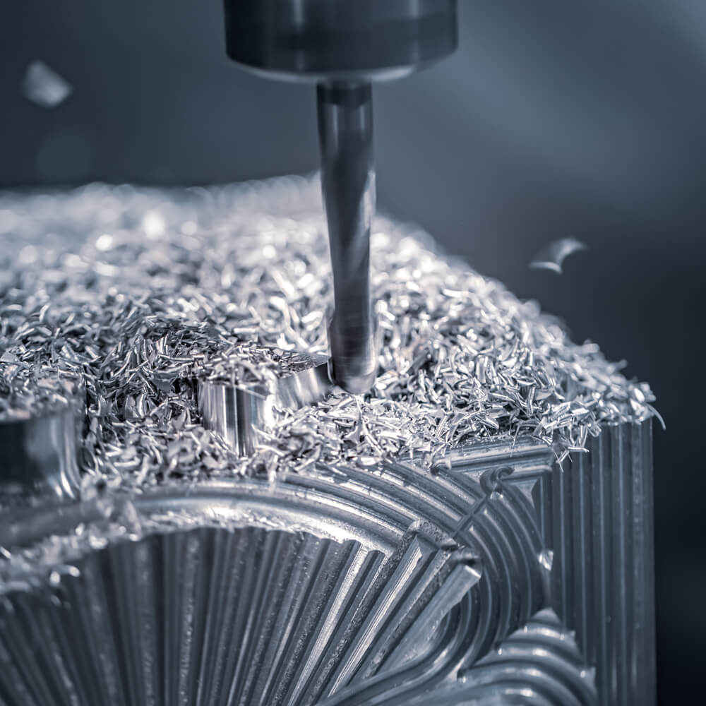
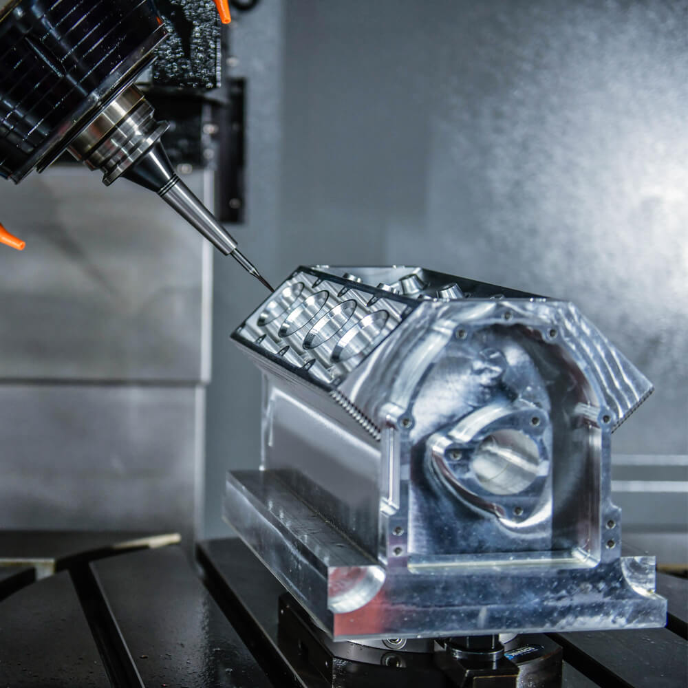
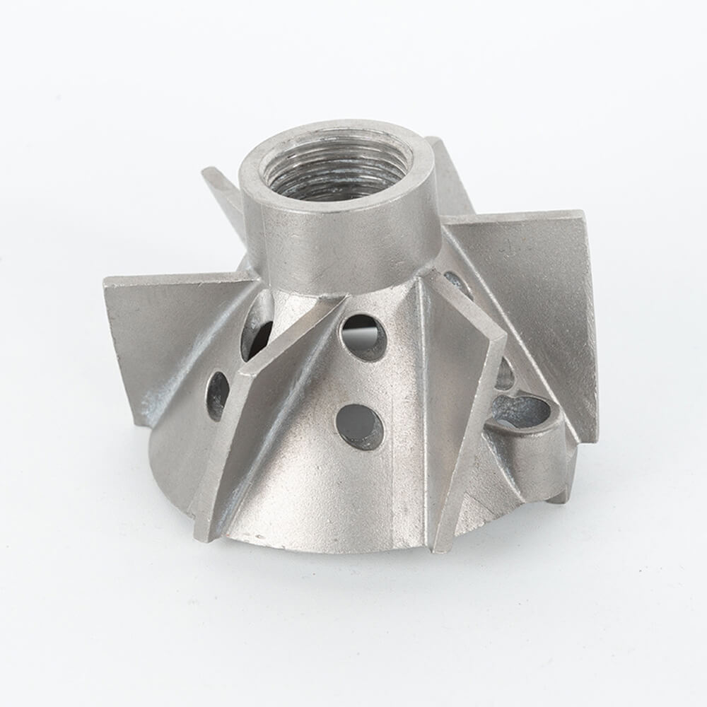
Ultra-High Precision Manufacturing for the Semiconductor Industry

Machining the Dimensionally Critical, Ultra-Clean, and Chemically Resistant Components that Enable the Future of Wafer Fabrication—from Process Chamber Assemblies to Wafer Handling End-Effectors.

  • ISO 9001 Certified
  • Class 1000 Cleanroom Assembly
  • Expertise in Machinable Ceramics & Quartz
Semiconductor
Your Expert Partner for Sheet Metal Fabrication

Your Expert Partner for Semiconductor Equipment Components

The semiconductor industry is defined by its pursuit of the infinitesimal, demanding a level of precision, cleanliness, and material science that is unparalleled by any other field. Celerity Precision is a specialized manufacturing partner in Shenzhen, China, built from the ground up to serve the world’s leading semiconductor equipment manufacturers. We produce the ultra-high purity and dimensionally critical components that are the heart of wafer fabrication equipment (WFE). From machining complex gas distribution showerheads and ceramic wafer chucks to finishing vacuum chamber components and assembling end-effectors in a cleanroom, we have the specialized technology and contamination-control protocols to meet the sector’s extreme requirements.

We understand that innovation in chip manufacturing is a cycle of intense R&D and rapid scaling. Our services are designed to accelerate this cycle, providing fast-turn, high-precision prototypes of new process chamber designs. As you move to volume production, we provide a reliable, repeatable, and scalable manufacturing solution, ensuring that the nanometer-level precision and ultra-high purity of the prototype are perfectly replicated in every single component. We are more than a supplier; we are a foundational partner in building the next generation of semiconductor technology.

The Celerity Precision Advantage for Semiconductor Manufacturing

Ultra-High Precision & Sub-Micron Tolerances

Our temperature-controlled facility and state-of-the-art CNC and metrology equipment allow us to achieve the sub-micron tolerances and extreme flatness (e.g., λ/4) required for wafer chucks, showerheads, and optical components.

Expertise in Advanced & Technical Materials

We specialize in machining the difficult and exotic materials essential for semiconductor processes, including high-purity Alumina (Al2O3), Silicon Carbide (SiC), Quartz, Sapphire, and high-performance polymers like Vespel® and Teflon®.

Contamination Control & Cleanliness

We follow rigorous contamination control protocols, including multi-stage ultrasonic cleaning, Class 1000 cleanroom assembly, and specialized vacuum-sealed packaging to ensure your components arrive pristine and ready for integration.

5-Axis Machining for Complex Geometries

Our advanced 5-axis capabilities are critical for manufacturing components with complex internal channels and thousands of precision-drilled holes, such as gas distribution plates (showerheads) and cooling plates.

Rapid Prototyping for Equipment R&D

We know speed is critical in developing new process nodes. We deliver functional, high-precision prototypes in a matter of days or weeks, enabling your engineering teams to test, validate, and innovate faster.

One-Stop Solution for Vacuum Assemblies

We simplify your supply chain by providing a complete solution, from precision machining and specialized anodizing to final cleaning, cleanroom assembly, and leak testing of vacuum-compatible sub-assemblies.

From CAD Model to Cleanroom-Ready Component: Our Process

RFQ & DFM for Semiconductor Applications

Submit your CAD models and specifications. Our engineers provide a rapid quote and offer DFM feedback focused on machining challenging materials and achieving critical surface finish and cleanliness requirements.

Process Planning & Specialized Tooling

We develop a detailed manufacturing plan using specialized diamond tooling for ceramics and optimized toolpaths designed to minimize subsurface damage and material stress.

Ultra-Pure Material Sourcing & Certification

We procure certified, ultra-high purity (UHP) materials from approved suppliers and provide full traceability documentation to meet the stringent requirements of the semiconductor industry.

Precision Machining & Lapping

Your parts are expertly machined in a controlled environment. Critical surfaces then undergo precision lapping and polishing to achieve specified flatness and mirror-like surface finishes.

Multi-Stage Cleaning & Finishing

Components go through a multi-stage ultrasonic cleaning process with deionized water. Aluminum parts undergo specialized anodizing to create a durable, non-contaminating, plasma-resistant surface.

CMM Inspection & Cleanroom Packaging

All critical features are verified in our clean inspection lab using high-accuracy CMMs and optical comparators. Parts are then bagged, vacuum-sealed, and double-bagged in our cleanroom before shipping.

Developing the Next Generation of Wafer Processing Technology?

Let’s collaborate on the ultra-precise components that will define your competitive edge.

Key Manufacturing Services for the Semiconductor Industry

Your Expert Partner for Precision CNC Milling

5-Axis CNC Milling

The core technology for creating complex components like single-piece electrostatic chuck (ESC) bodies, process chamber liners, and gas distribution systems.

Custom CNC Machining Services in China

CNC Ceramic & Quartz Machining

Specialized diamond grinding and ultrasonic machining for creating insulators, wafer chucks, focus rings, and viewports from hard, brittle materials.

Precision Casting (Investment Casting) Services in China

Precision Grinding, Lapping & Polishing

Essential for achieving the extreme flatness, parallelism, and low Ra surface finishes required for wafer contact surfaces and vacuum seals.

Your Expert Partner for Precision CNC Turning

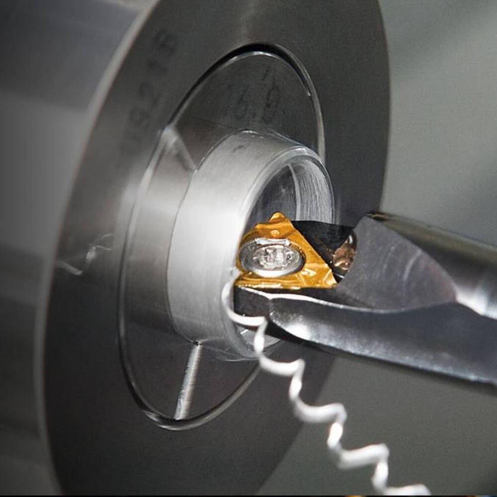
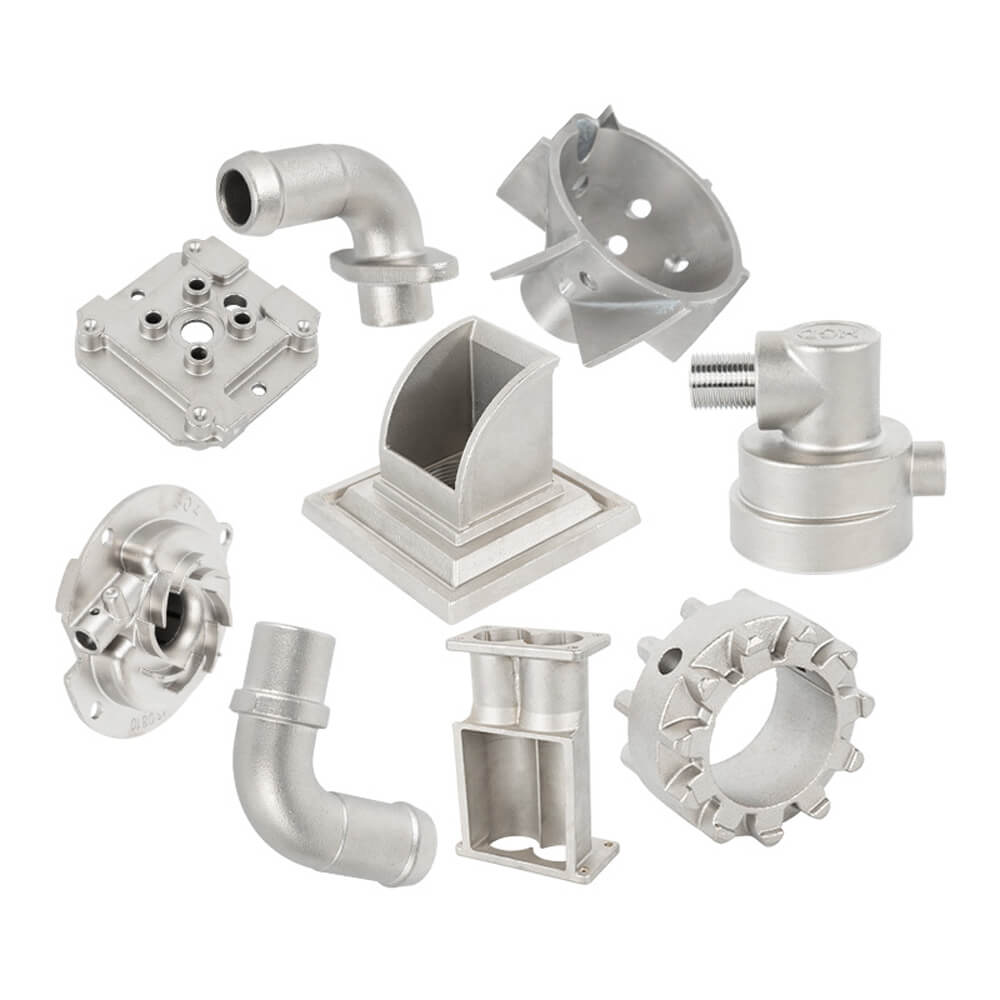
CNC Turning with Live Tooling:

Ideal for producing high-purity rings, pedestals, fasteners, and gas fittings from materials ranging from 316L VIM/VAR stainless steel to Vespel®.

TIG Welding (Gas Tungsten Arc Welding)

Specialized Anodizing

Providing Type III hardcoat anodizing that is optimized for vacuum compatibility, dielectric strength, and resistance to plasma etch processes.

Your Expert Partner for Precision Casting

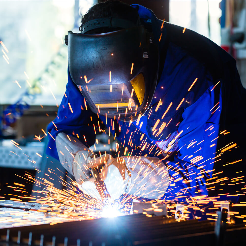
Cleanroom Assembly & Integration

Class 1000 cleanroom environment for assembling machined components, installing certified hardware, and performing helium leak testing on sealed modules.

High-Performance Materials and Finishes for Semiconductor Applications

Common Semiconductor-Grade Materials:

  • Alumina (Al2O3, 99.5%+)
  • Silicon Carbide (SiC)
  • Quartz & Fused Silica
  • Sapphire
  • Vespel® (SP-1)
  • Teflon® (PFA, PTFE)
  • PEEK
  • High-Purity Aluminum (6061-T6)
  • Stainless Steel (316L VIM/VAR)
PA (Nylon)
Electropolishing Surface Finish Supplier In China

Functional Surface Finishes:

  • Type III Hard Anodize (for plasma resistance)
  • Electropolishing (for UHP stainless steel parts)
  • Bead Blasting (with specified non-contaminating media)
  • Optical Polishing (down to <1 Ra)
  • Precision Cleaning (to Class 100 standards)

Gallery of Semiconductor Equipment Components

  • Gas Distribution Plates (Showerheads)
  • Wafer Chucks (Electrostatic, Vacuum, and Mechanical)
  • Process Chamber Liners and Components
  • Focus Rings, Edge Rings, and Clamp Rings
  • Ceramic Wafer Handling End-Effectors
  • Vacuum Chamber Bodies and Flanges
  • Insulators, Spacers, and Guides (Ceramic/PEEK)
  • Quartz Viewports and Plasma Tubes
  • Wafer Transfer Cassettes and Fixtures
  • Heater Pedestals and Lift Pins
Semiconductors

Frequently Asked Questions

Why are ceramics like Alumina and SiC used in semiconductor processing?

These materials offer extreme hardness, high thermal stability, and superior resistance to the highly corrosive plasma and chemical environments inside a process chamber, which would destroy most metals.

We use a multi-pronged approach: machining with specific coolants, rigorous multi-stage ultrasonic cleaning protocols, handling with powder-free gloves, and final inspection and packaging inside a certified cleanroom.

It is a critical component, typically made of aluminum or silicon, that looks like a showerhead with thousands of tiny, precisely drilled holes. It is used to introduce process gases uniformly across the surface of a silicon wafer.

Yes. We use a combination of precision milling and subsequent lapping/polishing processes to achieve the extreme flatness (often measured in microns or light bands) required for a wafer to be held uniformly by an electrostatic field.

Type III hardcoat anodizing is preferred. It creates a dense, non-porous, and durable ceramic-like layer that minimizes virtual leaks and outgassing, and it can withstand plasma environments much better than standard Type II anodizing.

Vespel® is a high-performance polymer that is strong, dimensionally stable at high temperatures, and does not generate particles. Crucially, it is soft enough that it will not scratch or damage the surface of a silicon wafer during handling.

While we don’t perform particle count testing in-house, our entire process—from cleaning to packaging—is designed to meet industry standards (e.g., Class 100). We can also work with third-party labs for specific cleanliness validation if required.

We use specialized diamond grinding wheels and tools on high-speed CNC machines with carefully controlled feed rates and coolant delivery. This allows us to accurately shape the material without introducing stress or subsurface damage.

For complex aluminum or stainless steel components, we can often deliver prototypes within 2-4 weeks. Parts made from technical ceramics may take longer due to material lead times and slower machining cycles.

VIM/VAR (Vacuum Induction Melting/Vacuum Arc Remelting) is a secondary melting process that produces a much cleaner, higher-purity steel with fewer impurities. This is critical for ultra-high vacuum (UHV) applications to minimize outgassing.

Related Ultra-Precision Applications

Medical

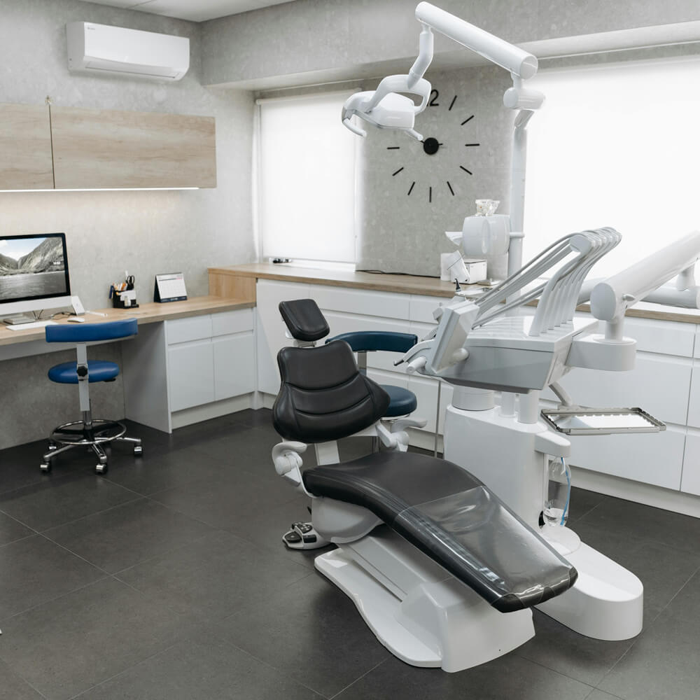
Medical & Healthcare

Manufacturing implants and surgical instruments where material purity, precision, and cleanliness are non-negotiable.

Consumer Electronics

Consumer Electronics

Creating the micro-mechanical components and precision assembly fixtures used to manufacture next-generation smartphones and devices.

Scientific Instruments

Scientific Instruments

Building components for mass spectrometers, electron microscopes, and vacuum systems that demand extreme precision and material stability.

Translate »
Scroll to Top

Request Your Quote!

Need something helped in a short time? We’ve got a plan for you.